Tata Electronics × Global Chip Companies: What Semiconductor Manufacturers Must Learn About India-Taiwan Packaging Collaboration
🔴 BREAKINGTata Electronics expands semiconductor packaging partnerships with global chip companies — India’s OSAT ambition accelerates◆India-Taiwan semiconductor collaboration signals shift in global chip packaging supply chains◆India Semiconductor Mission targets $100B electronics manufacturing by 2026 — packaging is the critical enabler◆Find verified semiconductor manufacturing partners on GTsetu — 100+ countries, zero commission◆🔴 BREAKINGTata Electronics expands semiconductor packaging partnerships with global chip companies — India’s OSAT ambition accelerates◆India-Taiwan semiconductor collaboration signals shift in global chip packaging supply chains◆India Semiconductor Mission targets $100B electronics manufacturing by 2026 — packaging is the critical enabler◆Find verified semiconductor manufacturing partners on GTsetu — 100+ countries, zero commission◆
Home › Blog › Tata Electronics × Global Chip Companies Collaboration
🔴 Breaking News💾 Semiconductor Packaging🇮🇳 India Manufacturing🇹🇼 Taiwan Tech Transfer
Tata Electronics × Global Chip Companies: How India-Taiwan Packaging Partnerships Are Rewriting the Semiconductor Map
India’s most ambitious electronics conglomerate is signing packaging partnerships with Taiwan-linked global chip companies — positioning India as a credible OSAT alternative to Malaysia and Vietnam. The strategic goal: capture a share of the $65B semiconductor packaging market by embedding India into global chip supply chains before 2027.
🎯 Direct Answer
Tata Electronics is expanding its semiconductor packaging partnerships with global chip companies, including firms headquartered or heavily integrated with Taiwan’s semiconductor ecosystem, to build India’s OSAT (Outsourced Semiconductor Assembly and Test) capabilities. These collaborations involve technology and manufacturing partnerships where global chip firms bring packaging know-how, IP, and customer relationships while Tata Electronics provides manufacturing infrastructure, India market access, and cost-competitive operations. This is part of a broader collaboration-led growth model that India is deploying to attract semiconductor ecosystems — moving beyond mere assembly toward advanced packaging formats like flip-chip, SiP, and heterogeneous integration. The partnerships directly support India Semiconductor Mission targets and position Tata Electronics as a Tier-1 OSAT player capable of serving global fabless chip designers.
📅 January 2026⏱ 16 min read✍️ GTsetu Editorial Team📰 Industry Analysis
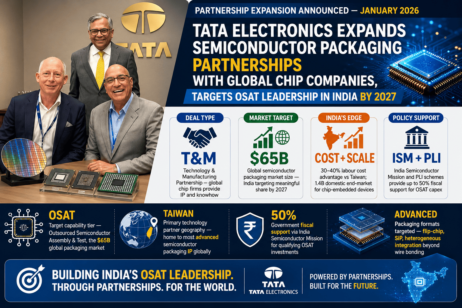
Deal Type
T&M
Technology & Manufacturing Partnership — global chip firms provide IP and knowhow
Market Target
$65B
Global semiconductor packaging market size — India targeting meaningful share by 2027
India’s Edge
Cost + Scale
30–40% labour cost advantage vs Taiwan; 1.4B domestic end-market for chip-embedded devices
Policy Support
ISM + PLI
India Semiconductor Mission and PLI schemes provide up to 50% fiscal support for OSAT capex
Section 1 — The News
1
The Full Story: Tata Electronics & Global Chip Packaging Partnerships
⬡
Partnership Expansion Announced — January 2026
Tata Electronics Expands Semiconductor Packaging Partnerships with Global Chip Companies, Targets OSAT Leadership in India by 2027
In January 2026, Tata Electronics — the Tata Group’s flagship electronics manufacturing entity and already India’s largest iPhone assembler — announced an expansion of its semiconductor packaging partnerships with multiple global chip companies, several of them deeply integrated with Taiwan’s world-leading semiconductor ecosystem.
Under these technology and manufacturing partnerships, global chip firms bring packaging IP, process technology, and customer access while Tata Electronics contributes manufacturing infrastructure, a cost-competitive Indian workforce, and proximity to one of the world’s fastest-growing end-markets for consumer electronics, automotive chips, and telecom devices. The strategic objective is to make India a credible Tier-1 OSAT destination capable of advanced packaging formats, not merely low-complexity wire bonding.
This move builds on Tata Electronics’ broader semiconductor ambitions — including its acquisition of a stake in Pegatron and its planned semiconductor fab collaboration — and represents a deliberate strategy of collaboration-led ecosystem building rather than attempting to replicate Taiwan’s decades of indigenous semiconductor development from scratch.
OSAT
Target capability tier — Outsourced Semiconductor Assembly & Test, the $65B global packaging market
Taiwan
Primary technology partner geography — home to most advanced semiconductor packaging IP globally
50%
Government fiscal support via India Semiconductor Mission for qualifying OSAT investments
“India is not trying to replicate Taiwan’s 40-year semiconductor journey in 10 years. We are taking a smarter path — building on partnerships, embedding ourselves into existing global supply chains, and letting collaboration accelerate what indigenous development alone cannot.”
— Industry Perspective on India’s Collaboration-Led Semiconductor Strategy
“Semiconductor packaging is the fastest entry point into the chip supply chain for India. It requires precision manufacturing capability, not fab-grade cleanrooms. And it is where global chip companies are most actively looking for supply chain diversification.”
— Semiconductor Industry Analyst, India Market Commentary 2026
💡 GTsetu Perspective
Tata Electronics is demonstrating what every Indian electronics manufacturer needs to understand: the fastest path into the global semiconductor supply chain is not to build fabs, but to become a world-class packaging partner. Semiconductor packaging is a $65B market where technology partnerships — not just capital — determine who wins. If Tata Electronics found its global chip partners, what Taiwanese, South Korean, or Dutch packaging technology partner could unlock your next tier of semiconductor customers? That is the question GTsetu helps you answer.
Section 2 — OSAT Capacity Roadmap
2
India’s OSAT Capacity Build — From Assembly Stronghold to Packaging Hub
Tata Electronics’ packaging partnerships do not exist in isolation — they are the technology backbone for India’s staged progression through the semiconductor value chain. The strategic logic is deliberate: secure packaging technology credibility first (via global chip partners), then scale capacity to meet the demand that credibility unlocks.
🏭 India OSAT Capability Progression — Tata Electronics
2022–23
Entry
iPhone Assembly EMS Tier
2024–25
Wire Bond Pkg
Basic Packaging ● Live
2026
Flip-Chip + SiP
Advanced Pkg In Progress
2027+
Heterogeneous Integration
Full OSAT Tier Target
⚙️ Why Technology Partnerships Must Precede Capacity Investment in Semiconductors
Tata Electronics’ packaging strategy illustrates a critical principle: in semiconductors, technology access and capacity expansion must be sequenced correctly. The partnerships with global chip companies upgrade the process sophistication and IP base of what Tata Electronics can produce, enabling them to compete for advanced packaging contracts that wire-bond-only players cannot win. Only then does scaling packaging capacity make financial sense — you need to know you can win and sustain the higher-margin contracts before committing the capital. Technology first, capacity second: always the right order for entering a new semiconductor tier.
Section 3 — The Anatomy
3
What Each Partner Brings to the Table
Like every successful semiconductor manufacturing collaboration, the Tata Electronics × global chip company partnerships work because each party contributes what the other cannot efficiently replicate. This complementarity principle is the foundation of any collaboration worth entering.
Process recipes, equipment specs, quality methodologies
Global chip partners’ knowhow runs on Tata’s hardware — no greenfield fab required
Market Access
India OEM & electronics ecosystem relationships
Global fabless and IDM customer relationships
Both parties unlock new customer pools for each other
Technology IP
Volume manufacturing discipline & cost efficiency
Advanced packaging process IP and yield optimisation
Tata produces to chip partners’ spec, elevating product to global OSAT standards
Quality Credentials
Existing quality systems proven with Apple supply chain
Chip-partner-validated process and reliability methodologies
Global chip partner endorsement de-risks Tata for procurement teams worldwide
Capital Commitment
Capex for packaging capacity expansion
Technical expertise, process documentation, no equity stake required
Asset-light for chip partners; high-value for Tata — asymmetric but balanced
Risk
Production risk, capex risk, yield ramp
Reputational risk — chip partner’s brand on Tata’s execution
Both sides have real skin in the game — different but consequential stakes
Section 4 — The Journey
4
Tata’s Semiconductor Journey — From iPhone Assembly to Chip Packaging
One of the most important strategic lessons from Tata’s semiconductor move is that the packaging partnerships are not a leap of faith — they are a logical extension of a proven electronics manufacturing capability. This is the right way to enter a new manufacturing segment: start with adjacent operations, prove execution at scale, then expand into higher-value processes using technology partnerships.
Tata Electronics begins iPhone assembly at Hosur, establishing India’s credibility as a precision electronics manufacturing location. Proves quality systems, cleanroom capability, and workforce scalability to Apple’s exacting standards — the most rigorous quality bar in consumer electronics.
2023–24
Pegatron Acquisition & Scale-Up
Tata acquires Pegatron’s India operations, significantly scaling assembly capacity and deepening Apple supply chain integration. Demonstrates ability to absorb and integrate Taiwanese electronics manufacturing knowhow — a direct precursor to semiconductor packaging partnerships.
2024–25
Basic Semiconductor Packaging Entry
Tata Electronics enters semiconductor packaging with wire bond and basic assembly capabilities, building foundational process knowledge. Begins qualifying with Indian electronics OEMs for domestic chip packaging demand, creating the commercial proof-of-concept for the advanced packaging push.
Jan 2026
Global Chip Company Packaging Partnerships Expansion
Building on proven EMS and basic packaging capabilities, Tata Electronics expands partnerships with global chip companies — many Taiwan-anchored — for advanced packaging formats including flip-chip, SiP, and heterogeneous integration. Technology partners bring packaging IP and customer access; Tata brings India manufacturing scale and cost. Target: Tier-1 OSAT capability capable of serving global fabless designers by 2027.
🔑 Key Lesson: Adjacency Is the Fastest Path to a New Technology Tier
Tata Electronics did not approach semiconductor packaging partners as a newcomer. Their proven iPhone assembly operations at Hosur — with Apple-grade quality systems and cleanroom discipline — were the credibility basis that made global chip companies take the packaging partnerships seriously. The advanced packaging collaboration is a logical extension of existing, proven electronics manufacturing capability. The fastest path to a high-value technology collaboration is almost always through an adjacent capability you have already proven. GTsetu’s platform helps you identify which of your existing manufacturing capabilities could become the credibility basis for a technology partnership in an adjacent semiconductor or electronics segment.
Section 5 — Why This Works
5
Why This Collaboration Model Works for Semiconductor Manufacturing
🎯 The Core Logic
Tata Electronics’ packaging partnership expansion succeeds because it is built on three interlocking strategic advantages: proven EMS credibility that makes global chip companies trust Tata’s execution quality; technology partnerships that directly unlock advanced packaging formats previously unavailable in India; and a market-timing alignment with global chip supply chain diversification driven by geopolitical risk reduction away from sole-source Taiwan dependence. Neither party could have achieved the same result independently — Tata Electronics cannot independently develop Taiwan’s decades of packaging IP, and global chip companies cannot manufacture in India at Tata’s cost structure.
Why India-Taiwan Semiconductor Collaboration Is Accelerating
China+1
Global chip companies’ supply chain diversification imperative — India is the beneficiary
$65B
Global semiconductor packaging market — India targeting 5–8% share by 2030
30–40%
India’s labour cost advantage vs Taiwan in packaging operations — critical for OSAT economics
ISM
India Semiconductor Mission provides 50% fiscal support for approved OSAT capex investments
1.4B
India’s domestic end-market — the world’s fastest-growing chip consumption base
6
India’s Semiconductor Packaging Opportunity — Why Now Is the Time to Collaborate
🇮🇳 India Semiconductor Manufacturing 2025–27
Why Every Global Semiconductor Company Should Be Exploring India’s Packaging Ecosystem Now
India’s electronics market crossed $150B in 2024. The government is backing semiconductor manufacturing with unprecedented policy support — 50% capital subsidy via the India Semiconductor Mission. Global chip companies are under geopolitical pressure to diversify supply chains away from Taiwan. And India’s domestic chip demand is growing at 15%+ annually as smartphones, EVs, and IoT devices proliferate. The timing for packaging collaboration is exceptional. The infrastructure — manufacturers like Tata Electronics — is ready and expanding.
$150B+
India electronics market 2024 — fastest-growing major electronics market globally
50%
Government capital subsidy for OSAT/packaging capex under India Semiconductor Mission
15%+
Annual growth in India’s domestic semiconductor consumption — demand is real and accelerating
$65B
Global OSAT market — Tata’s partnerships target a meaningful India-based share by 2027
Taiwan
Primary partner geography — concentration risk is driving global chip cos to India partnerships
30–40%
Cost advantage vs Taiwan in OSAT operations — fundamental economics drive India’s appeal
🌐 GTsetu for Semiconductor Collaboration
GTsetu’s verified partner network includes semiconductor packaging specialists, EMS providers, precision electronics manufacturers, substrate suppliers, and technology partners across India, Taiwan, South Korea, Japan, and 100+ other countries. Every company on GTsetu is verified on 6 government-sourced points: Name, Address, Registration Number, Company Status, Company Type, and Date of Certificate of Incorporation. Additional capabilities like OSAT certifications, cleanroom grades, and chip customer approvals are self-reported. If you’re a global semiconductor company looking to access India’s growing packaging ecosystem, or an Indian electronics manufacturer seeking technology partnerships for advanced packaging formats, GTsetu is where your partner search begins with verified profiles, not cold calls. Find semiconductor manufacturing partners →
Section 7 — Types of Collaboration
7
4 Types of Semiconductor Manufacturing Collaboration — Which Fits Your Situation?
Tata Electronics is using Technology & Manufacturing Partnerships for advanced packaging. But the right collaboration structure depends entirely on what you need, what you can invest, and how deeply you want to integrate. Here are the four primary models in semiconductor manufacturing.
01
Technology & Manufacturing Partnership
One party transfers packaging process IP and technical knowhow; the other manufactures. No new entity, no equity exchange. The Tata Electronics model. Fast to execute, lower risk, ideal when IP access and cost-competitive manufacturing are the specific complementary needs.
⚙️ Tata Electronics Model
02
Joint Venture (JV)
A new shared legal entity co-owned by both parties. Deepest integration, full profit and risk sharing. Best for long-term market anchor when both parties have large complementary assets — e.g. a global OSAT firm and an Indian conglomerate wanting a permanent India entity.
⚖️ Deep integration model
03
Contract Manufacturing / OSAT Outsourcing
You own the chip design and testing spec; an India-based OSAT partner packages to your specification for a per-unit fee. No equity sharing. Ideal for fabless chip designers wanting India packaging capacity without permanent commitment. Fully scalable and reversible.
🏭 Fabless chip designer model
04
Distribution & Sales Partnership
You supply packaged chips; a local distributor sells and provides technical support to India’s electronics OEMs. Lightest form of collaboration. Often the first step for a global chip company entering the India OEM supply chain before committing to local manufacturing.
🌍 Market entry, step 1
📊 Collaboration Model Comparison — Semiconductor Packaging
Model
Capital Required
Technology Access
Customer Credibility Uplift
Speed to Execute
Reversibility
T&M Partnership
Moderate (packaging capex)
✓ Full IP access
✓ High
Fast (6–12 months)
Moderate
Joint Venture
High — shared capex
✓ Co-developed IP
✓ Maximum
Slow (18–30 months)
Low
Contract OSAT
Minimal
~ Partial (process only)
~ Depends on OSAT certifications
Fastest (2–6 months)
High
Distribution
Minimal
✗ None
✗ Low
Fastest (1–3 months)
High
Section 8 — How to Collaborate
8
How to Collaborate: A 5-Step Playbook for Semiconductor Manufacturers
Tata Electronics’ packaging partnerships did not happen by accident. They followed a deliberate progression — from EMS credibility to basic packaging to advanced packaging collaboration — that every electronics and semiconductor manufacturer can adapt. Here is the distilled playbook.
1
Define Your Packaging Technology Gap with Precision
Tata Electronics knew exactly what they needed: advanced packaging process IP — flip-chip, SiP, heterogeneous integration — that wire-bond-only capability cannot support, plus the customer relationship credibility that global chip partners carry with fabless designers and IDMs. They didn’t need more assembly workers, they needed specific packaging knowhow and a door-opener to a new customer tier. Define your technology gap that precisely. Vague needs produce vague partner searches and failed negotiations.
2
Find Verified Technology Partners — Not Just Any Partner
The crucial word is “verified.” For manufacturers who don’t have an existing relationship to deepen, GTsetu provides verified profiles of packaging technology holders, OSAT specialists, substrate suppliers, and EMS partners across Taiwan, South Korea, Japan, Netherlands, and 100+ countries. GTsetu verifies companies using government tie-ups on 6 key points: Name, Address, Registration Number, Company Status, Company Type, and Date of Certificate of Incorporation. Additional information like packaging certifications, cleanroom grades, and OEM approvals is self-reported and should be validated independently through your own due diligence process.
3
Protect Your IP Before Any Technical Disclosure
In semiconductor packaging, your process recipes, test protocols, and bonding specifications are valuable IP. Before sharing anything sensitive — even a capability requirements document — execute a mutual NDA. This is non-negotiable regardless of how well you think you know the prospective partner. GTsetu’s built-in NDA workflow handles this automatically: mutual NDA executed and countersigned before any sensitive information is shared, with a full digital audit trail.
4
Choose the Right Collaboration Structure for Your Objective
Tata chose a Technology & Manufacturing Partnership for packaging — the right structure when you need IP access and customer credibility transfer without equity commitment. A JV is right when you want permanent shared ownership. A contract OSAT arrangement is right when you need packaging capacity without IP transfer risk. Match the structure to the objective, not to what’s easiest to negotiate. The structure determines your IP ownership, exclusivity, and exit options for the life of the agreement.
5
Formalise and Scale in Stages — Technology Qualification First, Capacity Second
Tata Electronics secured packaging technology partnerships and qualified processes before scaling packaging capacity investments. The technology partnership unlocks the market opportunity; the capacity investment capitalises on it. Never commit capital to scale production before you have the packaging IP, qualified processes, and customer relationships that will fill that capacity. Structure every collaboration milestone formally in writing: scope of technology transfer, fee structure, quality audit rights, exclusivity terms, and renewal conditions.
Section 9 — Dos and Don’ts
9
Dos and Don’ts of Semiconductor Manufacturing Collaboration
✅ Do These
✅ Build on adjacent proven capabilities — Tata’s iPhone assembly credibility opened packaging partnership doors
✅ Verify your partner’s actual chip customer references — the right partner opens fabless designer doors, not just provides process recipes
✅ Sequence technology qualification before capacity investment — qualify the packaging process, then scale the line
✅ Sign NDA before sharing packaging process specs, yield data, or test protocols
✅ Choose a partner whose chip customer relationships are complementary to yours — geographic and segment diversity
✅ Define the technology scope clearly — what packaging IP is transferred, on what terms, with what exclusivity
✅ Run a pilot packaging run (small batch qualification) before committing to capacity expansion capex
✅ Build in quality audit rights — technology provider must be able to verify process compliance and yield standards
✅ Use verified platforms like GTsetu rather than trade show introductions for strategic technology partners
✅ Document the collaboration formally — T&M agreement or licensing agreement before production begins
❌ Avoid These
❌ Invest in packaging capacity expansion before securing the technology and customer pipeline that will fill it
❌ Share process recipes, yield data, or packaging specs before NDA is countersigned
❌ Accept self-reported chip customer relationship claims without reference verification
❌ Assume packaging technology is transferable through documents alone — require resident engineers and process validation support
❌ Partner with a technology provider who is also your target customer’s current preferred OSAT supplier
❌ Neglect exclusivity terms — know whether your packaging technology partner can give the same IP to your competitors
❌ Choose a partner whose strengths duplicate yours — the technology gap is precisely where value is created
❌ Start production on informal terms — scope, fee structure, and IP ownership must be documented before production begins
❌ Underestimate cultural alignment requirements — India-Taiwan collaboration requires explicit technical communication protocols
❌ Build a JV when a Technology & Manufacturing Partnership achieves the same objective at lower commitment and risk
Section 10 — Misconceptions
10
Common Misconceptions That Kill Semiconductor Manufacturing Collaborations
❌ Myth
“India can build a semiconductor packaging industry from scratch — we don’t need technology partnerships.”
✅ Reality
Taiwan’s OSAT industry took 40+ years to build. The advanced packaging IP embedded in companies like ASE, Amkor Taiwan, and UTAC represents billions in R&D accumulated over decades. Tata Electronics is not trying to recreate this independently — they are licensing it through partnerships. Collaboration-led growth compresses a 40-year journey into a 5–7 year trajectory. That is precisely the strategic insight India is betting on.
❌ Myth
“We can clarify IP ownership and exclusivity terms after the first production runs.”
✅ Reality
In semiconductor packaging, process improvements develop rapidly after the first production runs. Once production has started on undefined IP terms, both parties’ leverage is gone. Joint process improvements — particularly yield optimisation discoveries — become disputed immediately unless ownership is pre-defined. Define IP ownership of jointly-developed improvements, exclusivity by geography and product segment, and improvement sharing terms before the first wafer is packaged.
A packaging technology partnership gives Tata Electronics technical credibility with global chip companies, not automatic supply contracts. The customer relationship transfer requires proactive commercial engagement, process qualification to the chip company’s spec, and often multi-lot test runs and reliability qualification. The technology partner’s endorsement is a door-opener, not a contract guarantee. Plan the commercial pursuit as a separate, parallel workstream from the technology transfer.
❌ Myth
“We should build OSAT capacity first to show chip companies we’re serious, then find technology partners.”
✅ Reality
Tata Electronics did the opposite — secured packaging technology partnerships first, then invested in scaling packaging capacity. Building OSAT capacity without the packaging IP and customer relationships to fill it is capital destruction. The correct sequence is always: technology partnership → process qualification → chip customer contracts → capacity expansion. Capital before pipeline is the most common mistake in semiconductor manufacturing entry.
❌ Myth
“A collaboration with a Taiwanese partner requires permanent physical presence in Taiwan to manage effectively.”
✅ Reality
Tata Electronics’ packaging partnerships are managed between India and Taiwan with structured engineering exchange programmes and process audit visits rather than permanent Taiwanese presence in India. What matters is clear protocols for process documentation transfer, scheduled engineering review sessions, and quality audit rights — not permanent physical proximity. GTsetu’s encrypted collaboration workspace supports exactly this structured cross-border technical working relationship.
Section 11 — GTsetu
11
How GTsetu Helps You Find the Right Semiconductor Collaboration Partner
Tata Electronics built its packaging partnerships through existing relationships and Apple supply chain connections. Most semiconductor and electronics manufacturers are not that fortunate — and even when an existing relationship exists, identifying whether it can be extended into advanced packaging requires systematic evaluation. GTsetu is the verified B2B manufacturing discovery platform that enables this evaluation at scale, across 100+ countries, before you reveal a single confidential detail.
🌐 Platform Spotlight — GTsetu
Find Verified Semiconductor Packaging Partners, OSAT Specialists, and Electronics Manufacturers Across 100+ Countries — Anonymously, Securely, With Zero Broker Fees
Every company on GTsetu is verified using government tie-ups on 6 key points: Name, Address, Registration Number, Company Status, Company Type, and Date of Certificate of Incorporation. This is the foundation of trust. Additional information such as packaging certifications, cleanroom grades, OEM approvals, and chip customer approvals is self-reported by companies. You evaluate who is real before you engage. You share nothing sensitive until an NDA is countersigned. And you pay no broker commission on any collaboration formed — the deal is entirely between you and your partner.
✅
6-Point Government-Sourced VerificationName, Address, Registration Number, Company Status, Company Type, Date of Incorporation confirmed using government tie-ups.
🕵️
Anonymous DiscoveryEvaluate verified partner profiles without revealing your identity until mutual interest is confirmed.
📄
Built-In NDA WorkflowShare packaging specs and process data only after NDA is executed — full audit trail, no external legal required.
🚫
Zero CommissionNo broker fees — your T&M partnership, JV, or OSAT contract is entirely between you and your partner.
🌍
100+ CountriesTaiwan, South Korea, Japan, Netherlands, India — find packaging technology partners in every semiconductor hub.
🔐
Encrypted CollaborationShare yield data, process specs, and engineering documentation securely between verified partners.
What Tata Electronics Did — What GTsetu Enables For You
What Tata Electronics Did
What GTsetu Enables for You
Why This Matters
Built on Apple supply chain credibility to earn trust from global chip packaging partners
✓ Browse verified company profiles with government-sourced verification before engaging
You evaluate the partner’s verified legal identity, not marketing claims
Chose partners for their advanced packaging IP and global fabless chip company access
✓ Filter by self-reported capabilities, certifications, and chip customer approvals (validate independently)
Find potential partners with the specific packaging IP and chip customer credibility your segment requires
Secured formal partnership documentation before beginning technology transfer
✓ Built-in NDA and document workflow protects IP from the first conversation
Your process recipes and packaging specs are protected at every stage
Targeted partners whose chip customer relationships were complementary (global vs India-domestic)
✓ Self-reported partner profiles show chip customer approvals and geographic coverage
Identify potential complementarity — the customer gap between your reach and theirs
Zero intermediary in chip partnerships — direct commercial terms with technology partners
✓ Zero commission on any partnership — all terms are direct between the two parties
No broker splits your margin or misaligns your commercial terms
FAQ
?
Frequently Asked Questions
Q
What exactly are Tata Electronics’ semiconductor packaging partnerships?
Tata Electronics has expanded its Technology & Manufacturing Partnerships with global semiconductor companies, particularly those integrated with Taiwan’s chip ecosystem, for the development and production of packaged semiconductors. Under these collaborations, global chip companies provide packaging process IP, engineering knowhow, and customer access while Tata Electronics contributes manufacturing infrastructure, cost-competitive Indian operations, and proximity to a massive domestic end-market. The partnerships target advanced packaging formats — flip-chip, System-in-Package (SiP), and heterogeneous integration — that go beyond basic wire bonding and position Tata as a Tier-1 OSAT capable of serving global fabless chip designers.
Q
What is OSAT and why is it strategically important for India?
OSAT — Outsourced Semiconductor Assembly and Test — refers to the back-end of semiconductor manufacturing: taking fabricated wafers from foundries (like TSMC) and packaging, assembling, and testing them into finished chips. The global OSAT market is approximately $65B. OSAT is strategically critical for India because it requires precision manufacturing capability, not the extreme capital intensity of a wafer fab ($10–15B per fab). OSAT is the fastest and most capital-efficient entry point into the semiconductor supply chain for India, requiring cleanrooms and precision assembly capability that India’s established electronics manufacturers — like Tata Electronics — already possess or are building. India’s government recognises this, providing 50% capital subsidies under the India Semiconductor Mission for qualified OSAT investments.
Q
What is the difference between a Technology & Manufacturing Partnership and a Joint Venture in semiconductors?
A Technology & Manufacturing Partnership is a service arrangement — no new entity, no equity exchange. One party provides packaging process IP and engineering knowhow; the other manufactures. It executes faster (6–12 months), requires less capital, and is easier to exit. A Joint Venture (JV) creates a new co-owned legal entity with shared equity, shared governance, and shared profits and losses. It takes longer (18–30 months to establish), requires higher capital, but provides deeper integration and full market ownership. For semiconductor packaging entry into India, a Technology & Manufacturing Partnership is typically the right first structure — it accesses the IP needed without the governance complexity of a JV, which can be added later once the relationship is proven.
Q
How can I find a Taiwanese or South Korean semiconductor packaging technology partner for my manufacturing business?
The systematic approach involves four steps: (1) Define your packaging technology gap precisely — what specific process formats, yield knowhow, or chip customer credibility do you need from a foreign partner? (2) Search verified platforms — GTsetu lists verified packaging specialists, OSAT firms, and technology holders across Taiwan, South Korea, Japan, and 100+ countries. GTsetu verifies companies on 6 points using government tie-ups: Name, Address, Registration Number, Company Status, Company Type, and Date of Certificate of Incorporation. Additional information like packaging certifications and chip customer approvals is self-reported and should be validated independently. (3) Evaluate anonymously first — review verified profiles before revealing your identity or requirements. (4) Execute NDA before any technical disclosure — GTsetu’s built-in NDA workflow handles this automatically. Cold approaches through trade shows rarely surface the right packaging technology partner; a structured, verified search on GTsetu does.
Q
What government support is available for semiconductor packaging investments in India?
India offers substantial policy support for OSAT and semiconductor packaging investments. The India Semiconductor Mission (ISM) provides up to 50% fiscal support on capital expenditure for qualifying semiconductor packaging and OSAT facilities. The Production Linked Incentive (PLI) scheme for IT Hardware provides additional incentives for electronics and semiconductor manufacturing. Several states — including Gujarat, Tamil Nadu, and Karnataka — offer supplementary state-level incentives including land at concessional rates, power subsidies, and expedited clearances. The combination of central and state incentives can materially reduce the effective capex for a packaging facility, making India’s economics competitive with Malaysia and Vietnam for mid-complexity packaging operations. GTsetu can connect you with verified Indian manufacturing partners who are already navigating these schemes.
Q
Does GTsetu charge commission on semiconductor partnerships formed through the platform?
No. GTsetu charges zero commission on any collaboration — whether a Technology & Manufacturing Partnership, Joint Venture, licensing agreement, contract OSAT arrangement, or distribution agreement — formed through the platform. The commercial terms of your agreement are entirely between you and your partner. Broker intermediation in semiconductor technology partnerships typically costs 5–15% of deal value and creates incentive misalignment. GTsetu removes the broker entirely. Learn more about GTsetu →
Ready to Find Your Semiconductor Packaging Partner? Start on GTsetu.
500+ verified manufacturers, OSAT specialists, packaging technology partners, and electronics manufacturers across Taiwan, South Korea, Japan, India, and 100+ countries. Zero broker fees. Anonymous discovery. Built-in NDA workflows. Your next semiconductor packaging collaboration starts with a verified profile — not a trade show handshake.
Business Development Expert | International Trade & Strategic Partnerships
Daniel Carter is a Business Development Expert at GTsetu, specializing in global trade, international business expansion, and strategic partnership development. With extensive experience working across multiple industries and markets, Daniel helps organizations identify growth opportunities, build commercial relationships, and expand their international footprint.
His expertise includes cross-border collaborations, market entry strategies, supply chain partnerships, manufacturing ecosystems, and business matchmaking. Through his work at GTsetu, Daniel supports companies seeking to establish meaningful connections with partners, distributors, investors, and industry stakeholders across global markets.
Daniel is committed to helping businesses unlock new opportunities through collaboration-driven growth and practical international trade strategies.