India × France Deep Tech Manufacturing Collaboration: What Semiconductor Manufacturers Must Learn About India-France Strategic Alliance
🔴 BREAKINGIndia × France Deep Tech Alliance: Bilateral semiconductor collaboration announced, targeting chip design, fab infrastructure, and joint innovation programs◆India’s semiconductor mission receives fresh bilateral momentum: France’s CEA-Leti and STMicroelectronics in focus◆India targets $100B semiconductor ecosystem by 2030 — bilateral deep tech partnerships are the engine◆Find verified electronics & semiconductor manufacturing partners on GTsetu — 100+ countries, zero commission◆🔴 BREAKINGIndia × France Deep Tech Alliance: Bilateral semiconductor collaboration announced, targeting chip design, fab infrastructure, and joint innovation programs◆India’s semiconductor mission receives fresh bilateral momentum: France’s CEA-Leti and STMicroelectronics in focus◆India targets $100B semiconductor ecosystem by 2030 — bilateral deep tech partnerships are the engine◆Find verified electronics & semiconductor manufacturing partners on GTsetu — 100+ countries, zero commission◆
Home › Blog › India × France Deep Tech Semiconductor Collaboration
🔴 Breaking News💡 Semiconductors & Deep Tech🇮🇳 India Manufacturing🇫🇷 France Tech Transfer
India × France Deep Tech: How Bilateral Innovation Programs Are Fuelling India’s Semiconductor Ambition
India and France have announced a landmark Strategic Alliance in deep tech manufacturing and semiconductors — combining France’s advanced microelectronics expertise with India’s engineering talent, scale, and growing fab infrastructure. The alliance targets chip design, advanced packaging, and joint R&D programs that place India on the global semiconductor map.
🎯 Direct Answer
The Governments of India and France have formalised a Strategic Alliance targeting deep tech manufacturing and semiconductor growth, announced in January 2026 and sourced from a PIB release. The bilateral collaboration focuses on chip design capability-building, advanced semiconductor fabrication infrastructure, joint R&D investment, and talent exchange programs — with France bringing its established microelectronics ecosystem (CEA-Leti, STMicroelectronics, Soitec) and India contributing engineering talent at scale, cost-competitive manufacturing, and the momentum of its India Semiconductor Mission backed by ₹76,000 crore in government incentives. This is not a standalone announcement — it deepens an existing bilateral innovation partnership that spans defence, space, and nuclear technology, making this a logical extension of a proven government-to-government relationship into the most strategically important industrial frontier of the 2020s.
📅 January 2026⏱ 16 min read✍️ GTsetu Editorial Team📰 Industry Analysis
Semiconductor ecosystem target by 2030, France alliance accelerates timeline
France’s Edge
CEA-Leti
World-leading microelectronics R&D institution; STMicro & Soitec in ecosystem
India Incentive
₹76,000 Cr
India Semiconductor Mission outlay backing domestic fab & design ecosystem
Section 1 — The News
1
The Full Story: India × France Deep Tech Manufacturing Alliance
⚡
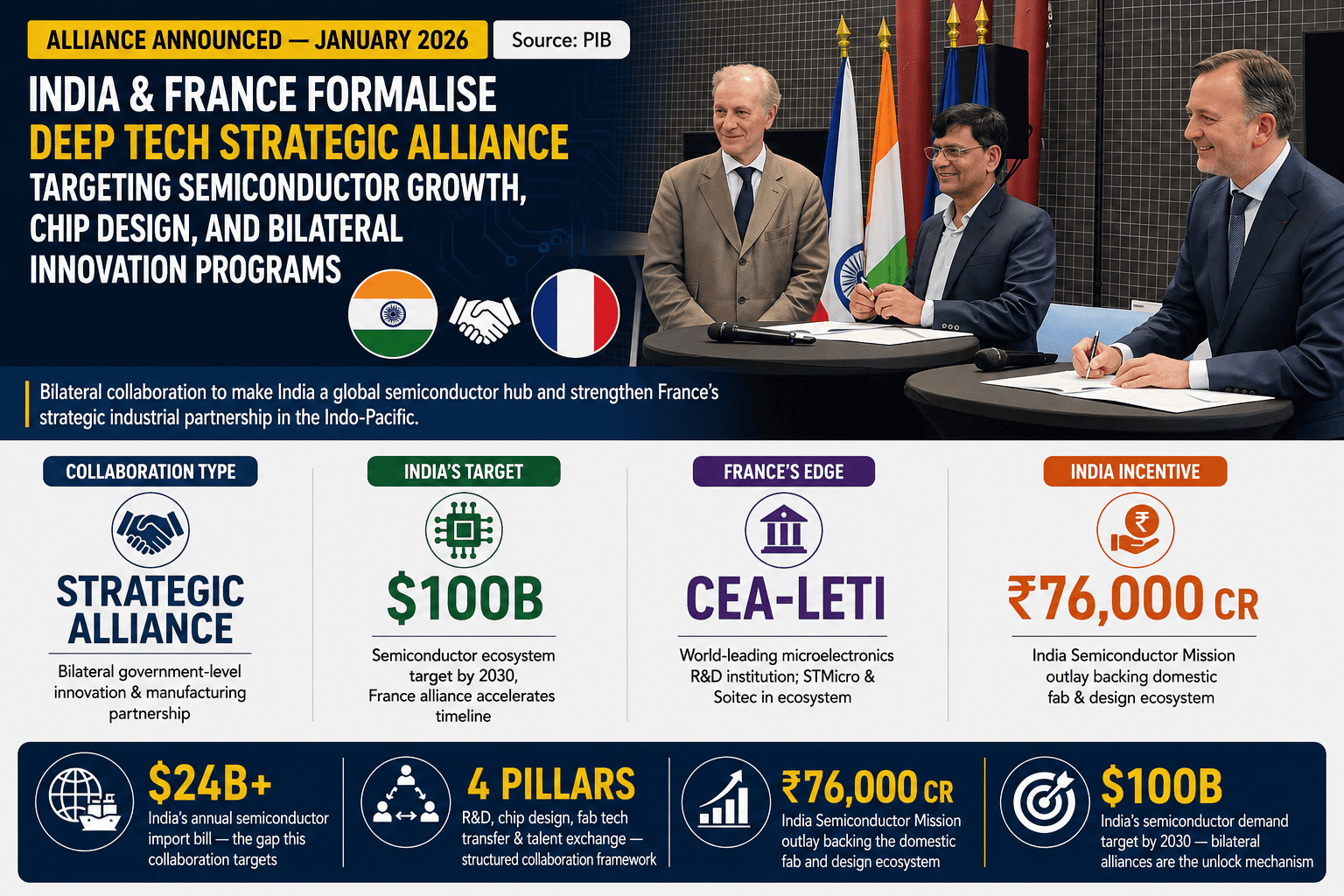
Alliance Announced — January 2026 | Source: PIB
India and France Formalise Deep Tech Strategic Alliance Targeting Semiconductor Growth, Chip Design, and Bilateral Innovation Programs
In January 2026, the Government of India and the Government of France announced a landmark Strategic Alliance in deep tech manufacturing and semiconductors — a bilateral collaboration designed to position India as a global semiconductor manufacturing hub while deepening France’s strategic industrial engagement in the Indo-Pacific region.
The alliance focuses on four critical pillars: joint semiconductor R&D investment, chip design ecosystem development in India, advanced packaging and fabrication technology transfer, and structured talent exchange programs between Indian engineering institutions and French microelectronics laboratories. France brings its globally recognised deep tech ecosystem — anchored by CEA-Leti, STMicroelectronics, and Soitec — while India contributes engineering scale, cost-competitive manufacturing infrastructure, and the policy momentum of the India Semiconductor Mission.
This collaboration is strategically timed: India’s semiconductor imports exceed $24 billion annually, domestic demand is projected to reach $100 billion by 2030, and the government has committed ₹76,000 crore to build a domestic semiconductor ecosystem. The France alliance unlocks critical technology transfer in chip design tools, silicon-on-insulator wafer technology, and advanced packaging — capabilities India cannot independently replicate at speed.
$24B+
India’s annual semiconductor import bill — the gap this collaboration targets
4 Pillars
R&D, chip design, fab tech transfer & talent exchange — structured collaboration framework
₹76,000 Cr
India Semiconductor Mission outlay backing the domestic fab and design ecosystem
$100B
India’s semiconductor demand target by 2030 — bilateral alliances are the unlock mechanism
“India and France share a natural strategic alignment in deep technology — France’s decades of microelectronics excellence combined with India’s engineering talent and manufacturing scale creates a bilateral complementarity that few other country pairs can match.”
— India-France Bilateral Innovation Program, PIB Release, January 2026
“Bilateral innovation programs are increasingly the primary mechanism through which industrial partnerships are formed — governments create the trust architecture, and the private sector executes on it.”
— GTsetu Industry Analysis, January 2026
💡 GTsetu Perspective
Government-to-government bilateral alliances are not abstract diplomacy — they are the operating framework within which private sector technology partnerships happen. When India and France formalise a deep tech alliance, it creates a permissive environment where CEA-Leti can share research with IISc, where STMicroelectronics can partner with Indian fabless design houses, and where capital flows in both directions without the friction of navigating uncharted bilateral territory. The private sector opportunity embedded in this alliance is enormous — but only companies who find the right verified partner and move quickly will capture it. If France found its India moment in semiconductors, which European technology partner could unlock your next product segment? That is the question GTsetu helps you answer.
Section 2 — The Four Pillars
2
Four Pillars of the India-France Semiconductor Collaboration
The Strategic Alliance does not sit as a single broad declaration — it is structured around four operational pillars, each targeting a specific gap in India’s semiconductor value chain. The strategic logic is precise: close the technology gap first, then build the manufacturing and talent infrastructure to sustain it.
🔬 Four Collaboration Pillars — India × France Deep Tech Alliance
Pillar 1
Joint R&D
Research Programs CEA-Leti × IISc
Pillar 2
Chip Design
Design Ecosystem ● Active
Pillar 3
Fab Tech Transfer
Advanced Packaging Scaling
Pillar 4
Talent Exchange
Engineers & PhDs Planned
⚙️ Why Technology Transfer and Infrastructure Must Be Sequenced Together
The India-France alliance illustrates a critical principle in deep tech collaboration: technology transfer and physical infrastructure investment must be sequenced correctly. The bilateral programs first upgrade India’s design and process capability through R&D collaboration, enabling Indian companies to compete for higher-specification semiconductor contracts. Only then does building fab capacity make commercial sense — you need to know you can win and fill those contracts before committing the capital to produce them. This sequence — technology capability first, physical scale second — is the right order for any manufacturer entering a new technology tier.
Section 3 — The Anatomy
3
What Each Partner Brings to the Table
Like every successful deep tech collaboration, the India × France alliance works because each party contributes what the other cannot efficiently replicate. This complementarity principle is the foundation of any collaboration worth entering.
Both parties unlock new supply chain positions for each other
Technology IP
Volume engineering scale & software development depth
Decades of microelectronics, SOI, MEMS, and photonics IP
India produces to French-validated specs, elevating product quality to global standards
Quality & Credentials
Existing ISO-certified design houses and ATMP units
CEA-Leti-validated process methodologies and standards
French endorsement de-risks India products for European procurement teams
Capital Commitment
₹76,000 Cr government incentive, private fab investment
Technical expertise and R&D co-investment
Asymmetric but balanced — France’s knowhow leverages India’s capital efficiently
Risk Profile
Production risk, infrastructure risk, capex risk
Reputational risk — French tech standards are on the line
Both sides have skin in the game — different but real stakes
Section 4 — The Relationship
4
A Layered Partnership — Defence to Space to Semiconductors
One of the most important strategic lessons from this alliance is that the India × France deep tech relationship is not new — it is a deepening of a proven bilateral partnership. Defence co-production, space collaboration, and nuclear technology cooperation preceded this semiconductor alliance. The same trust architecture that enabled Rafale jets enables chip design programs.
🤝 India × France — Bilateral Technology Partnership History
Phase 1
Defence & Aerospace Co-Production
India and France establish defence co-production including Rafale fighter jets and helicopter engine manufacturing. This builds bilateral trust, governance frameworks, and technology transfer precedents that underpin all subsequent collaborations.
2018–22
Space & Nuclear Technology Programs
Bilateral collaboration expands into space technology with ISRO-CNES programs and nuclear energy cooperation. France’s role as a trusted deep technology partner for India becomes institutionalised across multiple ministries and agencies.
2022–24
India Semiconductor Mission Launch + STMicro Fab Announcement
India launches its ₹76,000 Cr Semiconductor Mission. STMicroelectronics (French-Italian) announces a semiconductor ATMP unit in India in partnership with CG Power. This validates France’s private sector commitment to India’s semiconductor journey ahead of the government-level alliance.
Jan 2026
Strategic Alliance — Deep Tech & Semiconductor Growth
Building on the full bilateral relationship spanning defence, space, and nuclear, India and France formalise a comprehensive Strategic Alliance in deep tech manufacturing and semiconductors. Four pillars: joint R&D, chip design, fab tech transfer, and talent exchange. France’s CEA-Leti and India’s IISc anchor the research dimension. STMicroelectronics and Soitec anchor the industrial dimension. India’s semiconductor imports begin shifting toward domestic capability.
🔑 Key Lesson: Build on Proven Relationships
India and France did not launch a semiconductor alliance as strangers. They had already built governance alignment, technology transfer experience, and institutional trust through defence and space programs. The deep tech alliance was a logical extension — lower risk for France because they already knew India could execute complex technology programs; lower risk for India because they already knew France’s technology was real and transferable. The fastest path to a high-value collaboration is often through an existing one. GTsetu’s platform helps you identify which of your existing partner relationships could be expanded into new technology segments, and which new partners have the verified credentials to justify a first engagement.
Section 5 — Why This Works
5
Why This Collaboration Model Works for Deep Tech Manufacturing
🎯 The Core Logic
The India × France Strategic Alliance succeeds because it is built on three interlocking strategic advantages: an existing trusted bilateral relationship spanning defence and space, technology access that directly unlocks a previously inaccessible capability tier (advanced chip design and fab), and a market-timing alignment with India’s accelerating domestic semiconductor demand driven by electronics consumption and the global push to diversify chip supply chains beyond Taiwan and China. Neither party could have achieved the same result alone — India cannot independently develop France’s decades of CEA-Leti microelectronics IP, and France cannot manufacture in India at India’s cost structure.
Why India-France Deep Tech Collaboration Is Accelerating
$100B
India’s semiconductor demand target by 2030 — the largest untapped opportunity in global chip supply chain
China+1
Global chip supply chain diversification makes India the top alternative destination for semiconductor manufacturing
5M+
India’s STEM graduates annually — the talent base that makes India viable for chip design at scale
CEPA
India-EU trade framework and bilateral investment treaties ease technology transfer and IP flows
CEA-Leti
France’s world-leading microelectronics R&D lab — impossible to replicate; partnership is the only efficient access route
3 states
Gujarat, Karnataka, Odisha — approved semiconductor fab locations with state-level incentive stacks
Section 6 — India Semiconductor Opportunity
6
India’s Semiconductor Opportunity — Why Now Is the Time to Collaborate
🇮🇳 India Electronics & Semiconductor Market 2026–30
Why Every Global Deep Tech Supplier Should Be Entering India’s Semiconductor Ecosystem
India’s electronics market crossed $150 billion in 2024. The government is actively incentivising domestic semiconductor manufacturing through the ₹76,000 Cr Semiconductor Mission. EV adoption, 5G rollout, and defence electronics domestication are driving unprecedented semiconductor demand. The supply ecosystem — from fabless chip design houses to ATMP units — is being built in real time. The demand timing is exceptional. The France alliance provides the technology credibility that unlocks this entire value chain.
$150B+
India electronics market size in 2024, 3rd largest globally by growth rate
20%+
Annual growth rate of India’s semiconductor demand — fastest-growing major market
3 Fabs
Tata Electronics, CG Power/ST, and Kaynes Semicon — first wave of approved Indian fabs
150+
Fabless chip design companies in India — the France alliance upgrades their capability tier
French
IP ecosystem — the France alliance targets design and fab tech that India cannot build solo at speed
$24B
Annual semiconductor imports — every unit domesticated is an import substitution opportunity
🌐 GTsetu for Electronics & Semiconductor Collaboration
GTsetu’s verified partner network includes electronics manufacturers, semiconductor design houses, ATMP specialists, EMS providers, and technology partners across India, France, Germany, South Korea, Taiwan, and 100+ other countries. Every company on GTsetu is verified on 6 government-sourced points: Name, Address, Registration Number, Company Status, Company Type, and Date of Certificate of Incorporation. If you’re a European deep tech company looking to access India’s growing semiconductor supply chain, or an Indian design house seeking technology partnerships from France or Germany, GTsetu is where your partner search begins with verified profiles, not trade fair handshakes. Find electronics & semiconductor manufacturing partners →
Section 7 — Types of Collaboration
7
4 Types of Deep Tech Manufacturing Collaboration — Which Fits Your Situation?
India and France used a Strategic Alliance at the government level, but the private sector executes through multiple structures beneath it — from Joint Ventures and Technology Licensing Agreements to Contract R&D and Distribution Partnerships. The right structure depends entirely on what you need, what you can invest, and how deeply you want to integrate.
01
Strategic Alliance / MOU
A formal bilateral commitment to collaborate across a defined domain — technology, R&D, talent, and infrastructure — without creating a new equity entity. The India × France deep tech model. Fast to formalise, flexible in execution, ideal when the collaboration spans multiple programmes over multiple years.
🇮🇳🇫🇷 India × France (Semiconductors)
02
Technology Licensing Agreement
One party licenses patented IP or process technology to another for a fee or royalty — no new entity, no equity exchange. Fast to execute, lower risk. Ideal when IP access is the specific need and operational integration is not required. The private-sector equivalent of the government alliance framework.
⚖️ IP Access without Equity
03
Contract R&D / Joint Development
You define the specification; a partner R&D team develops the solution for a project fee. No equity sharing. Ideal when you need specific deep tech capability built without building an internal team. Scalable and fully reversible. STMicro and CG Power’s ATMP structure is a real-world example.
🔬 Capability without Headcount
04
Distribution & Channel Partnership
You manufacture or design; a local partner distributes and services in their market. The lightest form of collaboration. Often the first step before a deeper manufacturing or R&D agreement. Tests market demand before capital is committed. Ideal for European semiconductor companies entering India.
🌍 Market Entry, Step 1
📊 Collaboration Model Comparison — Deep Tech & Semiconductor Manufacturing
Model
Capital Required
Technology Access
OEM / Customer Credibility
Speed to Execute
Reversibility
Strategic Alliance
Low (program fees)
✓ Broad IP access
✓ Maximum
Moderate (6–12 months)
Moderate
Tech Licensing
Low (royalties)
✓ Full IP access
✓ High
Fast (3–6 months)
Moderate
Contract R&D
Minimal
~ Partial (output only)
~ Depends on partner credentials
Fastest (1–4 months)
High
Distribution
Minimal
✗ None
✗ Low
Fastest (1–3 months)
High
Section 8 — How to Collaborate
8
How to Collaborate: A 5-Step Playbook for Deep Tech Manufacturers
The India × France alliance did not happen by accident. It followed a deliberate progression — from trusted bilateral history to strategic technology alliance — that every semiconductor manufacturer and deep tech company can adapt. Here is the distilled playbook.
1
Define the Technology or Market Gap with Precision
India and France knew exactly what each needed: India required advanced chip design IP and microelectronics process knowhow; France needed access to India’s engineering talent and manufacturing scale. They didn’t need a new equity entity — they needed a structured program framework. Define your gap that precisely. Vague needs produce vague partner searches and failed negotiations. For private sector companies, this means specifying: which technology node, which process step, which customer segment you are targeting.
2
Find Verified Technology Partners — Not Just Any Partner
The crucial word is “verified.” France was not a random contact for India — it was a known partner with a documented track record. For companies who don’t have an existing relationship to deepen, GTsetu provides verified profiles of technology holders, EMS providers, ATMP specialists, and deep tech companies across France, Germany, South Korea, Taiwan, and 100+ countries. GTsetu verifies companies using government tie-ups on 6 key points: Name, Address, Registration Number, Company Status, Company Type, and Date of Certificate of Incorporation. Additional information like certifications and capability claims is self-reported and should be validated independently.
3
Protect Your IP Before Any Technical Disclosure
In semiconductor and deep tech, your chip architecture, process flows, EDA scripts, and design data are extremely valuable IP. Before sharing anything sensitive — even a capability requirements document — execute a mutual NDA. This is non-negotiable regardless of how well you think you know the prospective partner. GTsetu’s built-in NDA workflow handles this automatically: mutual NDA executed and countersigned before any sensitive information is shared, with a full digital audit trail. Governments use treaty-level agreements; your private-sector equivalent is a tight, bilateral NDA.
4
Choose the Right Collaboration Structure for Your Objective
India and France chose a Strategic Alliance for the government framework and are deploying multiple private-sector structures beneath it — licensing agreements, contract R&D, and JVs. A Strategic Alliance / MOU is right when you want a broad framework for multi-year collaboration. A Technology Licensing Agreement is right when you need specific IP access without equity commitment. A Contract R&D arrangement is right when you need a specific capability built without building internal headcount. Match the structure to the objective, not to what’s easiest to negotiate.
5
Formalise and Scale in Stages — Technology First, Infrastructure Second
The India-France alliance secured the technology collaboration framework first, then announced capacity investment milestones — in that order. The strategic alliance unlocks the capability opportunity; the infrastructure investment capitalises on it. Never commit capital to build fab capacity or design centres before you have the technology partnerships and customer commitments that will fill them. Structure every collaboration milestone formally in writing: scope of technology access, program timelines, IP ownership of jointly-developed outputs, audit rights, and renewal conditions.
Section 9 — Dos and Don’ts
9
Dos and Don’ts of Deep Tech Manufacturing Collaboration
✅ Do These
✅ Build on existing bilateral relationships — India-France extended proven defence trust into semiconductors
✅ Verify your partner’s customer and institutional references — the right partner opens procurement doors
✅ Sequence technology access before infrastructure investment — win the contracts, then build for them
✅ Sign NDA before sharing chip architecture, process parameters, or design databases
✅ Choose a partner whose customer relationships are complementary — France had European OEMs; India had Asian scale
✅ Define IP scope clearly — which technology is being accessed, on what terms, with what exclusivity
✅ Run a technology pilot (small design or process run) before committing to full fab investment
✅ Build in quality and compliance audit rights — technology provider must verify outputs meet their standards
✅ Use verified platforms like GTsetu rather than conference introductions for strategic deep tech partners
✅ Document the collaboration formally — MOU, licensing agreement, or JV agreement before any technology is shared
❌ Avoid These
❌ Invest in fab or design centre infrastructure before securing the technology partnerships to fill it
❌ Share chip architecture or process specifications before NDA is countersigned
❌ Accept self-reported customer or certification claims without independent reference verification
❌ Assume a partner’s technology is transferable without active knowledge-sharing — require engineers, not just documents
❌ Partner with a technology provider who is also your primary customer’s existing preferred supplier
❌ Neglect exclusivity terms — know whether your technology partner can give the same IP to your competitors
❌ Choose a partner whose strengths duplicate yours — the gap is where deep tech collaboration value is created
❌ Start production or R&D on informal terms — scope, fee structure, and IP ownership must be documented first
❌ Underestimate cultural alignment — India-France collaboration requires explicit communication protocols and timeline expectations
❌ Build a JV when a Technology Licensing Agreement would achieve the same objective at lower commitment and risk
Section 10 — Misconceptions
10
Common Misconceptions That Kill Deep Tech Manufacturing Collaborations
❌ Myth
“A bilateral government alliance has nothing to do with private sector opportunities — it’s just diplomacy.”
✅ Reality
Government alliances are the operating framework within which private sector technology partnerships happen. The India-France semiconductor alliance creates the legal, trade, and IP transfer environment that makes it practical for CEA-Leti to collaborate with IISc, for STMicro to invest in India, and for French fabless companies to source from Indian design houses. The private sector opportunity is embedded in the government framework — and companies who move first capture it.
❌ Myth
“India isn’t ready for advanced semiconductor manufacturing — you need to wait for infrastructure to mature.”
✅ Reality
Three fab projects are already approved and under construction. 150+ fabless design houses are operational. The India Semiconductor Mission is actively disbursing incentives. The window to enter is open now — infrastructure is being built around early entrants. Companies who wait for “maturity” will find the best partnerships and customer slots already taken by those who moved during the build phase.
❌ Myth
“The technology partner’s institutional relationships automatically become our commercial relationships.”
✅ Reality
The France alliance gives India technical credibility with European semiconductor customers, not automatic contracts. The commercial relationship transfer requires proactive business development, demonstrated capability to European standards, and often joint audits. France’s endorsement is a door-opener, not a guarantee. Plan the commercial pursuit strategy separately from the technology access program.
❌ Myth
“We should build the fab first to show customers we’re serious, then find the technology partner.”
✅ Reality
India did the opposite — secured the France alliance and institutional partnerships, then committed capital to fab and ATMP infrastructure. Building capacity without the technology backing and customer pipeline to fill it is capital destruction. The correct sequence is always: technology access → credibility → customer pipeline → capacity. Never invest in physical scale before you have the commercial and technology partnerships to justify it.
❌ Myth
“A collaboration with a French partner requires physical presence in France to manage the relationship effectively.”
✅ Reality
The India-France collaboration is managed with structured program visits and institutional liaisons rather than permanent physical presence. What matters is clear protocols for IP documentation transfer, scheduled technical review sessions, and quality audit rights — not permanent proximity. GTsetu’s encrypted collaboration workspace supports exactly this structured cross-border working relationship between Indian and European partners.
Section 11 — GTsetu
11
How GTsetu Helps You Find the Right Deep Tech Collaboration Partner
India had France through decades of bilateral history. Most deep tech companies are not that fortunate — and even when an existing relationship exists, identifying whether it can be extended into a new technology segment requires systematic evaluation. GTsetu is the verified B2B manufacturing discovery platform that enables this evaluation at scale, across 100+ countries, before you reveal a single confidential detail.
🌐 Platform Spotlight — GTsetu
Find Verified Electronics & Semiconductor Partners, Deep Tech Companies, and EMS Providers Across 100+ Countries — Anonymously, Securely, With Zero Broker Fees
Every company on GTsetu is verified using government tie-ups on 6 key points: Name, Address, Registration Number, Company Status, Company Type, and Date of Certificate of Incorporation. This is the foundation of trust. Additional information such as quality certifications (ISO 9001, IATF 16949, IEC standards), customer lists, manufacturing capabilities, and trade references is self-reported by companies. You evaluate who is real before you engage. You share nothing sensitive until an NDA is countersigned. And you pay no broker commission on any collaboration formed — the deal is entirely between you and your partner.
✅
6-Point Government-Sourced VerificationName, Address, Registration Number, Company Status, Company Type, Date of Incorporation confirmed using government tie-ups.
🕵️
Anonymous DiscoveryEvaluate verified partner profiles without revealing your identity until mutual interest is confirmed.
📄
Built-In NDA WorkflowShare chip designs and process specs only after NDA is executed — full audit trail, no external legal required.
🚫
Zero CommissionNo broker fees — your licensing agreement, JV, or supply contract is entirely between you and your partner.
🌍
100+ CountriesFrance, Germany, South Korea, Taiwan, India — find technology partners in every semiconductor and deep tech hub.
🔐
Encrypted CollaborationShare chip specs, EDA files, and process documentation securely between verified partners.
What India-France Did — What GTsetu Enables For You
What India-France Did
What GTsetu Enables for You
Why This Matters
Built on proven bilateral history spanning defence and space to extend trust into semiconductors
✓ Browse verified company profiles with government-sourced verification before engaging
You evaluate the partner’s verified legal identity, not marketing claims
Chose France for their world-class microelectronics IP (CEA-Leti, SOI, MEMS) and European OEM influence
✓ Filter by self-reported capabilities, certifications, and customer approvals (validate independently)
Find potential partners with the specific IP access and customer credibility your segment requires
Secured formal alliance documentation before beginning technology programs
✓ Built-in NDA and document workflow protects IP from the first conversation
Your chip architecture and design IP are protected at every stage
Targeted a partner whose technology relationships were complementary (European vs Asian)
✓ Self-reported partner profiles show customer approval lists and geographic market coverage
Identify potential complementarity — the gap between your customer reach and theirs
Zero intermediary in the collaboration — direct bilateral commercial terms
✓ Zero commission on any partnership — all terms are direct between the two parties
No broker splits your margin or misaligns your commercial terms
FAQ
?
Frequently Asked Questions
Q
What exactly did India and France agree to in the deep tech semiconductor collaboration?
India and France announced a Strategic Alliance in deep tech manufacturing and semiconductors in January 2026, sourced from a PIB release. The bilateral collaboration is structured around four pillars: joint semiconductor R&D programs, chip design ecosystem development in India, advanced packaging and fabrication technology transfer, and structured talent exchange between Indian engineering institutions and French microelectronics laboratories. France’s contribution is anchored by institutions and companies including CEA-Leti, STMicroelectronics, and Soitec. India’s contribution is anchored by the India Semiconductor Mission (₹76,000 Cr government backing), IIT and IISc engineering ecosystem, and rapidly growing ATMP and fabless design industry.
Q
Why is France specifically a strategic partner for India in semiconductors?
France holds a unique position in the global semiconductor ecosystem that few countries replicate. CEA-Leti is one of the world’s foremost applied microelectronics research labs, with proprietary IP in silicon-on-insulator (SOI), MEMS, photonics, and 3D chip integration. STMicroelectronics (Franco-Italian) is a top-10 global semiconductor company with existing India investments. Soitec is the world’s dominant manufacturer of SOI wafers. This ecosystem gives France both the R&D depth and the industrial presence to translate alliance commitments into real technology transfer. Combined with France’s existing bilateral trust with India — built through defence (Rafale) and space (ISRO-CNES) programs — it is a natural and credible deep tech partner.
Q
What is the difference between a Strategic Alliance and a Joint Venture, and when should I use each?
A Strategic Alliance is a formal bilateral commitment to collaborate across a defined domain — without creating a new equity entity. It is the right structure when collaboration spans multiple programs, multiple years, and multiple types of activity (R&D, talent, trade). It executes faster, requires lower capital, and is more flexible. A Joint Venture creates a new co-owned legal entity with shared equity, shared governance, and shared profits and losses. It is right when you want permanent shared ownership and full operational integration in a specific market or product. The India-France alliance uses a Strategic Alliance at the government level, with JVs and licensing agreements deployed at the private sector level beneath it. In practice, the alliance creates the conditions that make private-sector JVs and licensing agreements lower-risk and faster to execute.
Q
How can I find a French or European deep tech partner for my semiconductor or electronics business?
The systematic approach involves four steps: (1) Define your technology gap precisely — which specific process IP, design capability, or institutional credibility do you need from a European partner? (2) Search verified platforms — GTsetu lists verified manufacturers, design houses, EMS providers, and technology companies across France, Germany, South Korea, Taiwan, and 100+ countries. GTsetu verifies companies using government tie-ups on 6 points. Additional information like certifications and capabilities is self-reported and should be validated independently. (3) Evaluate anonymously first — review verified profiles and capability data before revealing your identity or technical requirements. (4) Execute NDA before any technical disclosure — GTsetu’s built-in NDA workflow handles this automatically before any sensitive document exchange. Conference introductions and LinkedIn rarely surface the right technology partner; a structured, verified search on GTsetu does.
Q
What happens if my technology partner also provides the same IP to my competitors?
This is one of the most important and most frequently overlooked questions in deep tech collaboration. If your technology partner provides the same IP to your direct competitors, your collaboration advantage disappears. Before signing any alliance, licensing agreement, or technology program: (1) Exclusivity scope — is the technology exclusive to you in your geographic market or product segment? (2) Competitive supply terms — can the technology provider work with competitors during your agreement period? (3) Jointly-developed improvement ownership — who owns process improvements developed together during the collaboration? These terms must be in the agreement before signing. In government-level alliances, exclusivity is typically handled through industry-specific program structures that channel technology into defined priority sectors rather than blanket restrictions.
Q
Does GTsetu charge commission on technology licensing or cross-border partnerships formed through the platform?
No. GTsetu charges zero commission on any collaboration — whether a Strategic Alliance MOU, Technology Licensing Agreement, Joint Venture, Contract R&D arrangement, or distribution partnership — formed through the platform. The commercial terms of your agreement are entirely between you and your partner. This is a foundational design principle: broker intermediation in deep tech and semiconductor partnerships typically costs 5–15% of deal value and creates incentive misalignment between the broker and both parties. GTsetu removes the broker entirely. Learn more about GTsetu →
Ready to Find Your France? Explore Cross-Border Partnerships on GTsetu.
500+ verified manufacturers, deep tech companies, semiconductor design houses, EMS providers, and ATMP specialists across France, Germany, South Korea, Taiwan, India, and 100+ countries. Zero broker fees. Anonymous discovery. Built-in NDA workflows. Your next electronics and semiconductor collaboration starts with a verified profile — not a trade fair handshake.
Business Development Expert | Global Trade & Cross-Border Partnerships
Lui Wang is a Business Development Expert at GTsetu, specializing in international trade, cross-border partnerships, and market expansion strategies. With extensive experience working across diverse business ecosystems, Lui helps companies identify growth opportunities, establish strategic collaborations, and navigate the complexities of global commerce.
His expertise spans manufacturing, supply chain partnerships, technology collaborations, market entry strategies, and international business development. Through GTsetu, Lui works closely with businesses, trade organizations, and industry stakeholders to facilitate meaningful connections that drive sustainable growth across regions and sectors.
Lui is particularly passionate about helping organizations build long-term international partnerships, unlock new markets, and strengthen their global competitiveness in an increasingly interconnected economy.